FDTD Solver
Solver Physics: The numerical method of computational electrodynamics that provides approximate solutions to the system of Maxwell's equations is known as Finite-Difference Time-Domain (FDTD). It is also referred to as Yee's method, named after Kane S. Yee, a Chinese-American applied mathematician. As a time-domain method, FDTD handles nonlinear material properties in a rather natural way and can cover a wide frequency range by running only a single simulation.
Features Description: Adds or sets FDTD simulation region and boundary conditions.
Notes : When FDTD solver is selected, user cannot add FDE solver and EME solver at the same time.
1 Tool bar
1.1 General tab
 |
|---|
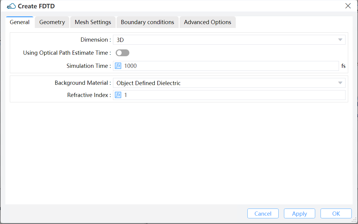
1) Dimension: Number of dimensions of the simulation region. (Default: 3D)
2) Using Optical Path Estimate Time: It is the switch button that the estimation of simulation time based on optical path.
3) Simulation Time: Simulation time indicates the maximum duration of the simulation to be implemented. In reality the simulation may end earlier when some of the auto-shutoff conditions are satisfied before running till this maximum simulation time. (Default: 1000 fs)
4) Background Material: The combo box allows user to set the background material from drop down menu. “Project”, “Object Defined Dielectric”, and “Go to Material Library” can be operated.
5) Project: The “Background Material” can be selected from the “Project” sublist in the “Material Database” based upon the needs.
6) Object Defined Dielectric: The object-defined dielectric material, a default setting if user forgets to set background material, is defined for the current object background material setting, and once the user chooses this option, he does not need to set any material from the standard, user, or project material database. And the object-defined dielectric will not be loaded into any material database.
Go to Material Library: If selected, user can go to standard material database to set background material according to needs. And the selected material relative property from standard material database will be displayed in the material data list.
7) Refractive Index: The refractive index of the surrounding, background medium in the simulation region.(Default: 1)
1.2 Geometry tab:
 |
|---|
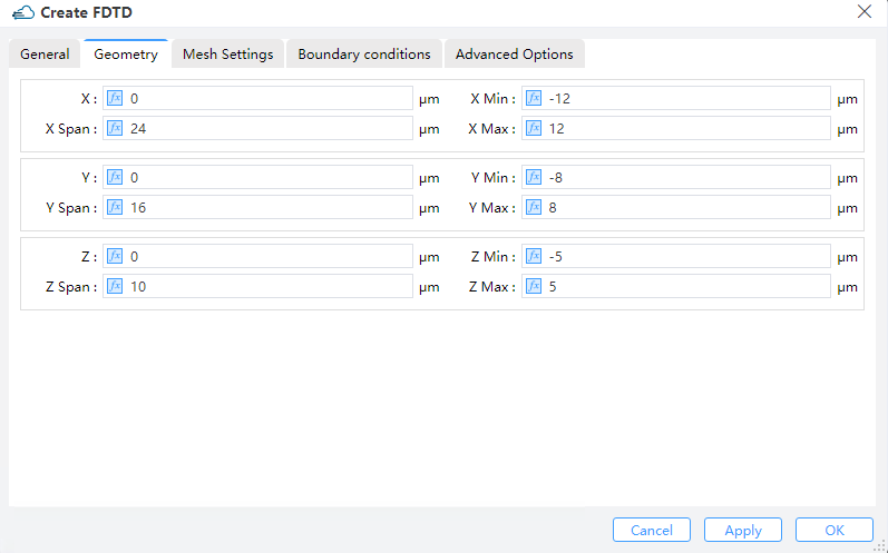
1) X, Y, Z: The center position of the simulation region.
2) X Min, X Max: X min, X max position.
3) Y Min, Y Max: Y min, Y max position.
4) Z Min, Z Max: Z min, Z max position.
5) X Span, Y Span, Z Span: X, Y, Z span of the simulation region.
1.3 Mesh Settings tab:
 |
|---|
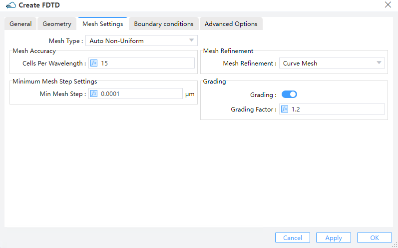
1) Mesh Type: Algorithms for generating the mesh are available, to be explained as follows:
① Auto non-uniform (Default): By default, a non-uniform mesh is generated according to the mesh accuracy.
② Uniform: A uniform mesh is used over the whole simulation region, disregarding any material properties. An override region forces the specified mesh size everywhere instead of inside the override region only, whenever it is used together with this option.
2) Mesh Accuracy: Mesh Accuracy indicates the number of cells per wavelength. (Default: 15).
3) Minimum Mesh Step Settings: Minimum Mesh Step indicates the absolute minimum grid size inside the entire solver window.
4) Mesh Refinement: Select an approach to calculate refined mesh properties.
① Staircase: Any point inside a Yee cell might be evaluated to determine of which material it is consisted, and the properties for that single material are used for depicting the E field at that point. As a consequence, the discretized structure hardly accounts for structure variations that arises inside a single Yee cell, therefore leading to a “Staircase” permittivity grid which agrees exactly with the Cartesian grid. Besides, all layers are effectively shifted to the closest E field position inside the Yee cell, implying that there is no way for the thickness to be resolved as finer than dx.thickness cannot be resolved to better than dx.
② Curve Mesh: Effective permittivities can be derived via a contour path recipe, which effectively takes the dielectric interface shapes, as well as material weight inside a cell into account.
③ Grading: The Grading factor specifies the biggest ratio of the neighboring spatial grids. (Default: 1.2)
1.4 Boundary Conditions tab:
 |
|---|
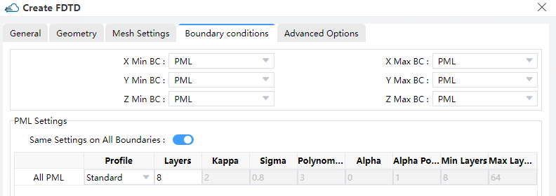
1) PML: A PML (Perfectly Matched Layer) mimics in essence an ideally open (or reflectionless) boundary upon which is designed to absorb all the incident electromagnetic waves with impedance matched materials to eliminate reflections.
2) PEC: PEC boundary conditions are introduced to mimic boundaries that behave exactly like a Perfect Electric Conductor (PEC). Metal boundaries reflect all the electromagnetic waves, and hence no energy can get through a simulation volume bounded by metals, simulating ideal metal boundaries, such as metal waveguide, reflector antenna, etc.
3) Symmetric/Anti-Symmetric: The Symmetric or Anti-Symmetric Boundary condition is used for reducing simulation time by the Electromagnetic fields which is symmetric through the middle plane of the simulation region. The specific selection between “Symmetric” and “Anti-Symmetric” is according to the relationship of source polarization and symmetric plane. If the normal of symmetric plane is tangential to source polarization, choose the “Symmetric” option. Otherwise, choose the “Anti-symmetric” option.
4) PML settings: The properties of every PML boundary can be set separately. However if the state of the Same Settings on All Boundary Conditions is enabled, all PML boundaries will possess the same profile by sharing the common properties in the table, including “Layers”, “Kappa”, “Alpha”, “Sigma”, “Polynomial”, “Alpha Polynomial”, “Min Layers”, and “Max Layers”. And you can also customize the PML Boundary in Profile,which concludes “Custom” and “Standad” two selections.
5) X/Y/Z min/ max PML: These fields describe the boundary conditions to be applied along the perimeter of the simulation region.
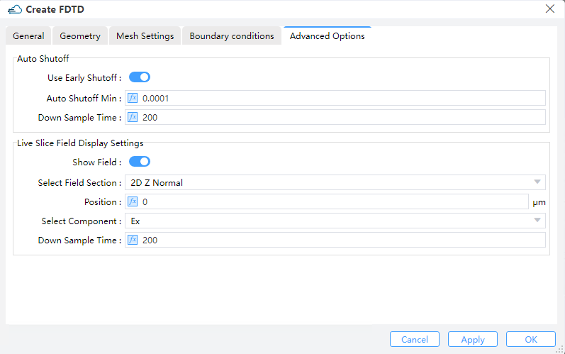
1.5 Advanced Options tab:
 |
|---|
1) Auto Shutoff : Stops the simulation when the energy in the simulation goes below the “Auto Shutoff Min” when the “Use Early Shutoff ” state is on , you can set min auto shutoff (Default: 1e-4) and down sample time (Default: 200)
2) Down sample time: Under the dt time step down sampling, check whether satisfying the auto shutoff conditions. (Default: 200, and 10 <= it <= 1000)
3) Live Slice Field Display Settings
① Show Field: Real-time filed slice display switch. (Default: on)
② Select Field Section: Combo box allows you to choose from a list of 2D planes normal to the axes for field display. ( 2D Z Normal by default)
③ Position:The position of slice (0 μm by default)
④ Select Component:Combo box allows you to choose from a list of the existing field components ( Ex by default)
⑤ Down sample time: The time step down sampling for displaying field.(200 fs by default)